Smart Materials and Sensors: Atomistic to Macro Physics Models
The miniaturization of micro-electro-mechanical systems incorporating the sensors, actuators, and electronic circuitry for signal processing and control feedback has been made possible by advances in technologies originating in the semiconductor industry. The integration of the micro-electro-mechanical system, inter-digital transducers, and conformal antenna in the multifunctional smart materials results in an intelligent system suitable for sensing and control of a variety of functions in automobile, aerospace, marine, medical and civil structures. A good understanding and prediction of the performance of the smart materials plays a critical role in the developments of such intelligent systems. This requires an accurate modeling of smart material behaviors at the nano/microscales.
Multiscale modeling of thermo-electro-mechanical material behavior
Piezoelectricity refers to the property of producing an electric field when the material is subjected to an external force. A ferroelectrics is a piezoelectric material in which a spontaneous polarization can be reoriented. Piezoelectric or ferroelectric materials are widely used in engineering applications, including sensors and actuators, capacitors and memory applications. They are the most popular smart materials.
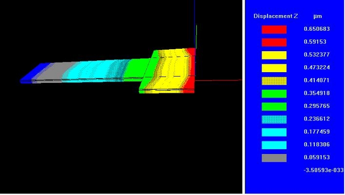
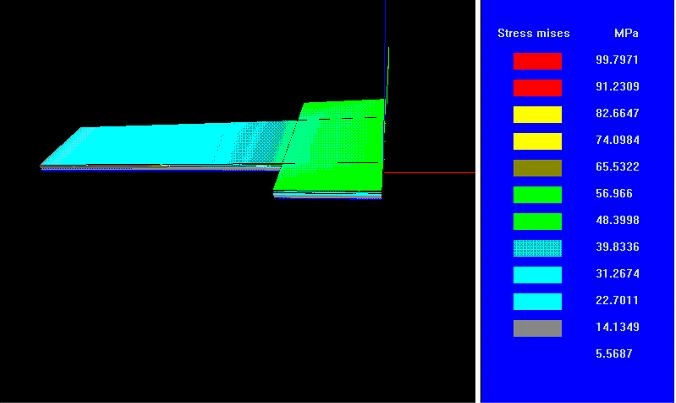
We have developed a multiscale model of ferroelectrics, which can describe the effect of atomic displacement at the sub-nano scale, domain motion from nano- to microscale, and simulate a fully coupled thermo-electro-mechanical response of the material. Shown in Fig.1 and Fig.2 is a PZT four-layer cantilever-resonator after simulation-based structural optimization.
 |  |
| Fig. 1: Deformation of the four-layer (SiO2, Pt, PZT, Pt) resonator under electric field | Fig. 2: Stress distribution of the four-layer (SiO2, Pt, PZT, Pt) resonator under electric field |
Multiscale modeling of polycrystalline material
Most industrial materials are polycrystalline materials, which are composed of randomly oriented crystallites, and a critical role is often played by the grain boundaries. The effect of grain size and grain boundaries on the material response becomes significant as the size of device goes to the microscale or nanoscale.
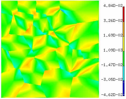
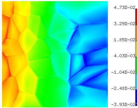
We have been developing a multiscale model of polycrystalline material to simulate the material behavior that incorporates all the relevant length and time scales ranging from the atomic-level, via the microstructural length and time scale, to the continuum level. Fig.3 and Fig.4 are the computer results of thermal stress distribution due to initial process temperature and due to temperature gradient, respectively. Those results indicate the inhomogeneous material response and are very close to microscopic experimental observations on polycrystalline materials.
 |  |
| Fig. 3: Thermal Stress distribution in polysilicon due to initial process temperature | Fig. 4: Thermal Stress distribution in polysilicon due to temperature gradient |

